 Purdue
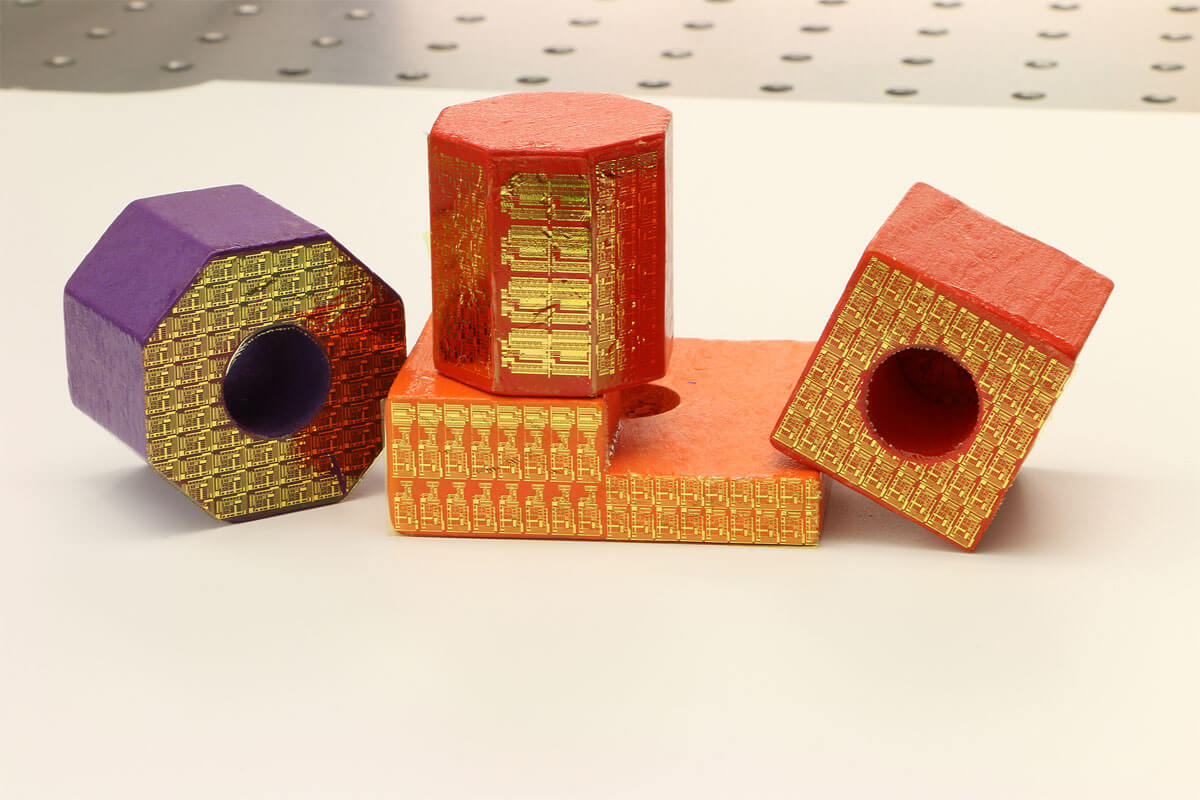
Electronic Stickers Take the Internet of Things One Step Further
The thin-film electronic circuits can be used on objects to make them smart.
According to Purdue University, the network of the Internet of Things (IoT) is expanding day by day, thanks to smartphones, medical devices and machine parts that continue to turn into wireless sensors with the advancement in technology. Every single day, we see new objects being connected to the internet and this, in turn, is also significantly enhancing the intelligence behind the technology.
Now, there is yet another innovation where the researchers at the University of Virginia and the Purdue University have collaborated on a project to develop a method of fabrication. This method enables thin-film and tiny electronic circuits to peel and stick from a surface. Thanks to this technique, not only the manufacturing steps are eliminated,but it also enables an object to be able to sense the environment it is in and be controlled via a high-tech sticker that works through an application.
The Purdue Assistant Professor of Mechanical Engineering and Biomedical Engineering, Chi Hwan Lee commented on the possibilities of this method saying, “We could customize a sensor, stick it onto a drone, and send the drone to dangerous areas to detect gas leaks, for example.”
Another fantastic application of these stickers can also be initiating wireless communication.
The majority of the electronic circuits that we see today are built on silicon “wafer.” It is a rigid and flat substrate. This wafer has the capability to withstand chemical etching and high temperatures that are necessary to eliminate the circuits from the confines of the wafer. However, this etching and high temperatures usually damage the wafer. This is why it becomes pertinent for the manufacturers to adjust their process and try to accommodate a new wafer every single time.
However, the new fabrication technique designed by Lee and his team, which is also called “transfer printing,” utilizes one wafer to build an infinite number of films that can hold the electronic circuit. Also, they do not use chemicals or high temperatures. On the contrary, the film easily peels off at room temperature by using energy-saving water.
Lee explains, “It’s like the red paint on San Francisco’s Golden Gate Bridge – paint peels because the environment is very wet. So in our case, submerging the wafer and completed the circuit in water significantly reduces the mechanical peeling stress and is environmentally friendly.”